

How To Draw Transistor Level Circuit
From Transistors to Functions
For the purpose of this course, we volition consider transistors to be the bones building blocks of figurer hardware.
A transistor is an electronic device that has three ends: a source, a sink, and a gate. The effigy below shows three private transistors (circa 1960s). Today'south engineering science allows united states of america to pack up to i million transistors per square millimeter (circa 2006). An Intel processor measuring less than a square inch has well over 1.v billion transistors on it (circa 2007) -- more than data available hither.
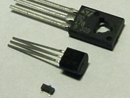
Effigy 1: Picture of individual transistors (courtesy of Wikipedia).
More conveniently, transistors are depicted using the picture below.
Figure two: Symbol used to describe a transistor with its three connectedness points.
Transistors as Faucets!
The operation of a transistor could be explained by making an analogy to faucets.
Simply like a transistor, a faucet is connected to a source (the water visitor), the faucet drains in a sink, and the flow of h2o through the faucet is controlled by a gate (the knob). If the faucet knob (gate) is turned ON water flows from the source to the sink, otherwise if the faucet knob (gate) is turned OFF no water flows.
Figure 3: Faucet Functioning: The gate controls the period of water from source to sink.
If we represent the fact that water flows from the source to the sink with a ane (or ON) and the fact that water does non flow from the source to the sink with a 0 (or OFF), we can understand how a transistor works but by changing "h2o" to "electricity". In item:
-
When the gate of a transistor is ON (or has a value 1) so electricity flows from the source to the sink and the transistor is said to be ON
-
Otherwise when the gate of a transistor is OFF (or has a value 0) so electricity does not flow from the source to the sink and the transistor is said to be OFF.
The current applied science used to build figurer hardware (fries) is called CMOS, which stands for Complementary Metal�Oxide�Semiconductor.
In CMOS, in addition to using the transistor described above, we use another kind of transistors, which is turned ON when the gate is OFF and is turned OFF when the gate is ON. In other words, its functioning is "complementary" (or contrary) to the one nosotros just described above. The symbol for this complementary type of transistors is shown below. The symbol is quite similar to the transistor we described to a higher place, except for the "bubble" connected to the gate. This chimera means that this transistor works in the opposite way (it'due south ON when the gate is OFF and OFF when the gate is ON.
Effigy 4: Symbol used to depict a complementary transistor.
To behave the analogy with faucets, one tin can think of a faucet that lets h2o period from the source to the sink when its knob is tightened but not when the knob is loosened.
Using Transistors to Build Bigger Circuits
Using transistors equally building blocks, we tin build larger circuits that perform interesting (logical) operations.
Our start instance is the Not circuit. The figure below shows how to connect two transistors together to build an inverter (also known as a NOT gate).
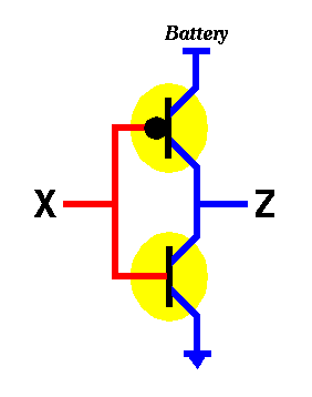
Effigy v: An inverter circuit (known as the NOT gate).
Now, let's find out what the inverter excursion above volition practice when presented with an input (i.e. Ten). Nosotros know that 10 tin take ane of ii values, either 0 or 1. Allow'due south study each one separately.
-
If X=0 then past definition of the bottom transistor, it volition be OFF, which means that electricity will not be able to flow from its source to its sink. Likewise, by definition, the tiptop transistor will be ON, which ways that electricity will exist able to flow from its source to its sink. The question is, will there be any electricity coming out from Z (where Z is the output of that circuit). The answer is YES. Since the top transistor is ON and the bottom transistor is OFF, electricity flowing out of the battery will go through the top transistor merely will not be able to make it through the bottom ane. In other words, it will menstruum out through Z. To visualize the operation of the inverter, it may exist helpful to think about this example using the water analogy discussed before.
-
If X=1 then by definition of the bottom transistor, it will be ON, which means that any electricity already available at its source will drain in the sink. Also, by definition, the top transistor will be OFF, which means that no electricity will be able to catamenia from its source to its sink. The question is, volition there be any electricity coming out from Z (where Z is the output of that circuit). The answer is NO. Since the peak transistor is OFF and the bottom transistor is ON, electricity flowing out of the battery will be blocked past the top transistor and any electricity that may exist in Z, volition drain. In other words, at that place will be no electricity flowing out through Z. Again, it may be helpful to think nearly this case using the water illustration discussed before.
The table below sums up the operation of the NOT gate by providing an output (Z) for every possible input (X) of the excursion. Tables like this one (providing usa with the value of a function for all possible combination of inputs of that function) are called truth tables.
Figure 6: Truth table summarizing operation of the inverter circuit (the NOT function).
The effigy below shows how one could build another circuit using transistors. This circuit has two inputs 10 and Y and one output Z.
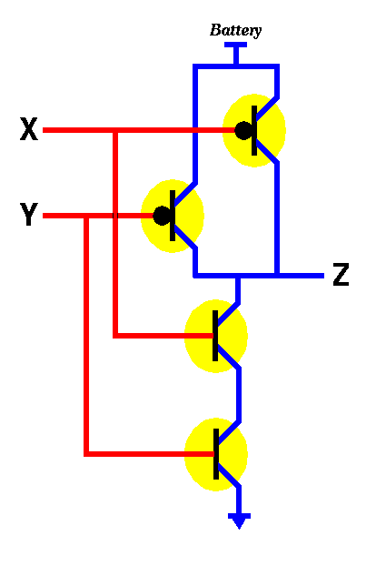
Figure seven: The "not both X and Y" circuit (the NAND part).
There are iv possibilities for the inputs, namely
- X=0, Y=0
- X=0, Y=1
- X=1, Y=0
- Ten=i, Y=one
Let's endeavor to do an analysis similar to what we did for the Not gate. In particular, consider the case when both X and Y are 0. By definition, the bottom two transistors will be OFF while the meridian ii volition be ON thus allowing electricity to flow from the battery to the output Z. Thus for X=0, Y=0 we get Z=1. In the instance when both X and Y are one, the bottom two transistors volition be ON while the elevation two will be OFF, thus no electricity volition menses from the bombardment to the output Z. Thus for X=1, Y=1 we become Z=0. In the case when X=0 and Y=i, we discover that one of the 2 acme transistors volition be ON and the other will be OFF. Similarly, for the lesser transistors, one will be ON and the other will be OFF. Thus, electricity volition nonetheless be able to flow to Z (through the ON transistor on top), thus making Z=1. The case for X=1, Y=0 is similar. It yields Z=1.
Thus nosotros become the truth table below for the excursion shown to a higher place.
NAND
| X | Y | Z |
| 0 | 0 | 1 |
| 0 | 1 | 1 |
| 1 | 0 | one |
| 1 | 1 | 0 |
Effigy eight: Truth table summarizing functioning of the NAND gate.
The in a higher place truth table says that the output of the circuit is 0 only when the ii inputs are i this is exactly the reverse of the AND logical role (the AND logical function outputs 1 whenever both its beginning input AND its second input are 1). Thus we call this circuit the "Not AND" gate or the NAND gate.
In order to build an AND gate, all we take to do is to connect the output of the NAND gate to the input of a Non gate.
Effigy 9: The "both X and Y" circuit (the AND role).
Like to the NAND gate nosotros can build a NOR (Non OR) gate as shown in the figure beneath.
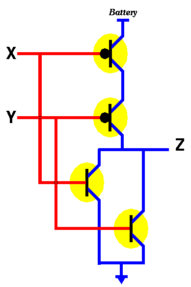
Effigy x: The "not X nor Y" circuit (the NOR function).
We leave it as an exercise to cheque that the truth table for the to a higher place excursion is every bit shown beneath.
NOR
| 10 | Y | Z |
| 0 | 0 | 1 |
| 0 | one | 0 |
| 1 | 0 | 0 |
| i | i | 0 |
Figure 11: Truth table summarizing operation of the NOR gate.
And, just as we were able to obtain the AND function by connecting the output of the NAND function to the input of the Non part (encounter figure ix), we tin can obtain the OR role (which outputs 1 whenever at least 1 of its inputs is 1) by connecting the output of the NOR role to the input of the Not function.
Basic Logic Functions
From the in a higher place examples and word, we conclude that we tin construct the main logic functions AND, OR, and Non using transistors.
Since we will exist using these functions (or gates) in time to come designs, nosotros will give them symbols so that we don't have to depict all the transistors and all the connections each time we want to use (say) an OR gate.
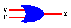
For an OR gate we will employ the symbol below:
OR
| 10 | Y | Z |
| 0 | 0 | 0 |
| 0 | ane | one |
| one | 0 | i |
| 1 | ane | 1 |
Figure 12: Symbol of an OR gate and its truth tabular array.
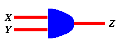
For an AND gate nosotros will utilise the symbol beneath:
AND
| X | Y | Z |
| 0 | 0 | 0 |
| 0 | 1 | 0 |
| one | 0 | 0 |
| 1 | 1 | i |
Figure xiii: Symbol of an AND gate and its truth table.
Finally, for the Not gate we will apply the symbol below:
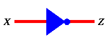
Figure 14: Symbol of a Non gate and its truth table.
Other Logic Functions
By putting AND, OR, and Not gates together, we tin can construct more than complex (logic) functions.
Allow's start with the elementary instance shown in the figure below-- namely, constructing a three-input OR gate out of two-input OR gates. Observe that the beliefs of the 3-input OR gate is to produce an output of 1 when at to the lowest degree one of the inputs is 1, otherwise (i.east. when all inputs are 0, it produces 0).
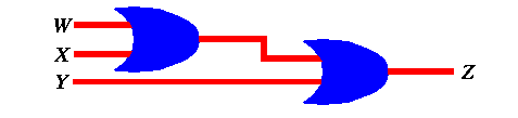
Figure 15: A 3-input OR function synthetic using 2 2-input OR gates.
This procedure could exist generalized thus assuasive us to build four-input, 5-input, etc.. OR gates.
Similarly, we tin can also construct AND gates with more than two inputs. For case the figure below shows two different means of implementing a 4-input AND gate from 2-input AND gates.
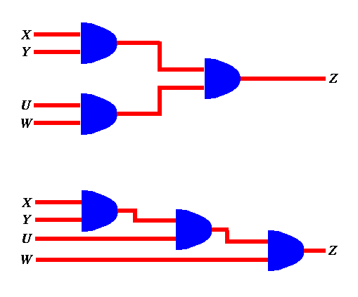
Figure xvi: A 4-input AND office constructed using 3 2-input AND gates.
The above 2 examples are uncomplicated, since 1 tin can predict the behavior of many AND gates connected together or the behavior of many OR gates connected together. By and large speaking, all the same, this may not be that unproblematic. Given an capricious circuit, we can find out what information technology does past amalgam its truth table , which is a tabulation of the circuit output for all possible input combinations. Take for example the excursion below.
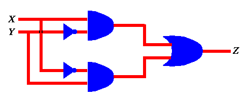
Effigy 17: A function constructed past connecting various AND, OR, and NOT gates.
First, nosotros notice that it has two inputs, X and Y. Each i of these inputs may presume one of two values 0 and 1. Thus the truth tabular array for that circuit will have four entries. For each such entry we accept to find out the output Z. Nosotros practice so by labeling the circuit.
For instance, if 10 = 0 and Y = 0 , we can label the various inputs and outputs of all gates until nosotros find out that Z = 0 as shown below.
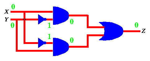
Effigy 18: Output of office in Effigy xv when X=0 and Y=0.
Similarly, we can practise it for 10 = 0 and Y = 1 to get Z = i as shown below.
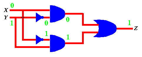
Figure xix: Output of role in Figure 15 when 10=0 and Y=one.
If nosotros do this for all 4 input combinations, we get the truth tabular array beneath.
XOR
| X | Y | Z |
| 0 | 0 | 0 |
| 0 | 1 | 1 |
| 1 | 0 | i |
| 1 | i | 0 |
Figure xx: Truth tabular array for role in Effigy 17 -- role is known every bit XOR.
Observe that the above process could be used to find out the truth table for any logical circuit.
From the truth table in Figure 20, we discover that the behavior of the circuit is such that it produces an output of 1 if both inputs are not the same --i.e., when either one of its inputs is 1 but not both. This office is called the exclusive or (XOR) function. The figure beneath shows the symbol used to depict the XOR function (or gate) shown in Figure 17.
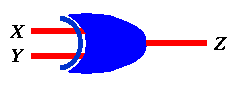
Effigy 21: Symbol of XOR gate.
Can you guess how many transistors it would take to build the above XOR gate?
To summarize, if we take transistors as a building block, one can see how to combine a handful of transistors to build logical functions such equally AND, OR, Not, XOR, etc. Past putting a few of these together we become fifty-fifty more than complex (interesting) functions, and the procedure goes on, allowing u.s. to build functionalities equally circuitous as those supported past (say) the processor in your PC.
Materials adapted from lecture notes by Azer Bestavros -- first developed for CS-101 in 1995.

Source: https://www.cs.bu.edu/~best/courses/modules/Transistors2Gates/
Posted by: scotttheatione.blogspot.com
0 Response to "How To Draw Transistor Level Circuit"
Post a Comment